
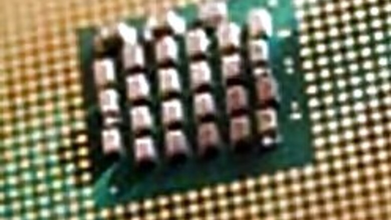
Washington: A scientist of Indian origin from MIT, along with colleagues and researchers from Texas Instruments (TI), has developed an energy-efficient microchip for portable electronics, which could lead to longer-lasting, self-charging cellphones and can be used on devices as varied as medical implants to sensors that detect enemy tanks..
The project was carried out by Anantha Chandrakasan, the Joseph F and Nancy P Keithley Professor of Electrical Engineering MIT; Joyce Kwong, a graduate student in MITs Department of Electrical Engineering and Computer Science (EECS), and colleagues from MIT and Texas Instruments.
This newly-developed chip design for portable electronics would be up to 10 times more energy-efficient than present technology. In fact, the design could lead to cell phones, implantable medical devices and sensors that last far longer when running from a battery.
The team demonstrated the ultra-low-power design techniques on TI’s MSP430, a widely used microcontroller. The work was conducted at the MIT Microsystems Technology Laboratories, which Chandrakasan directs.
The key to the improvement in energy efficiency was to find ways of making the circuits on the chip work at a voltage level much lower than usual, explained Chandrakasan.
"If semiconductor companies can overcome production obstacles, such a chip could be ready for commercial use in five years," he said.
While most current chips operate at around one volt, the new design works at just 0.3 volts. One key to the new design, was to build a high-efficiency DC-to-DC converter-which reduces the voltage to the lower level-right on the same chip, reducing the number of separate components, said Chandrakasan.
The redesigned memory and logic, along with the DC-to-DC converter, are all integrated to realise a complete system-on-a-chip solution, he added.
Chandrakasan says the researchers had to design new memory and logic circuits, and new computer tools will be needed to finish the job.
At lower power, imperfections in the silicon used to make chips become more noticeable, posing another hurdle to production. The researchers were scheduled to discuss their work Tuesday at a semiconductor conference in San Francisco.
PAGE_BREAK
According to Chandrakasan, commercial applications for this new microchip could become available in five years, maybe even sooner, in a number of exciting areas. For example, portable and implantable medical devices, portable communications devices and networking devices could be based on such chips, and thus have greatly increased operating times.
There may also be a variety of military applications in the production of tiny, self-contained sensor networks that could be dispersed in a battlefield. In addition, the technology could be suitable for body area networks or wirelessly enabled body sensor networks.
The research was funded by the US Defense Advanced Research Projects Agency. The Pentagon's research arm, known by the acronym DARPA, gave MIT about $700,000 over the past two years to conduct the research — and more will be awarded soon — said Barry S Perlman, an Army technology executive.
Perlman said power consumption is a key issue with battlefield sensor networks and the MIT work offers 'significant potential' to operate more sophisticated systems or run them longer.
"The future Army is very robotic," Perlman said. "The soldier controls what goes on, but (with sensors) he doesn't have to put himself in harm's way. It saves lives."


Comments
0 comment