
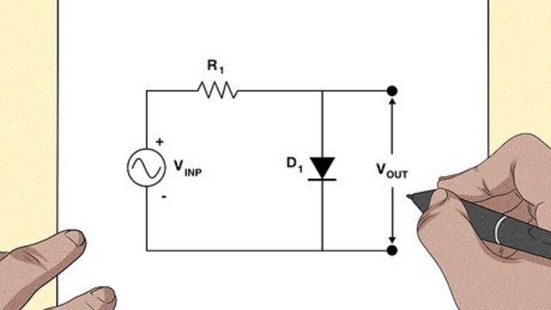
Understand the basic diode clipping circuits completely. Drawing the transfer characteristics for the circuit becomes easy, if you understand the circuit completely and able to get it's output waveform.
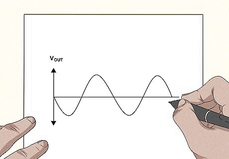
Examine the output waveform for the above circuit. Understand the output waveform of the circuit. Observe the Vref (reference voltage) line, which is in the positive X axis in the input waveform, also observe that above the Vref line, the output gets limited to Vref in the output waveform.
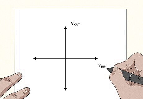
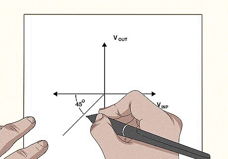
Transfer characteristics must be analysed for positive and negative input voltages. Since transfer characteristics is defined as the plot of Vinp (input voltage) versus Vout (output voltage), input voltage may be positive, negative or zero. Therefore, start the analysis for both types of inputs. Make a note of the output voltage obtained for the corresponding input voltage. Plotting becomes easy if you start analyzing the circuit from the negative input voltages (however, you can also start analysing from positive input voltages).
Analyse the circuit for negative input voltages. When the negative input voltage is applied to the circuit, diode (Ideal) becomes reverse biased. Hence, the circuit becomes open and no current flows through the circuit. Therefore, the output voltage at any point simply follows the input voltage at that point, without any modification. Plotting the graph of Vinp versus Vout in this condition results in a graph of straight line having a slope (defined as tan θ = Δ Vout/Δ Vinp) of 1 because, as Vinp changes, Vout also changes, but the amount of change in Vinp and Vout are equal at any point, as the output follows the input. Therefore Δ Vout = Δ Vinp = a (some value), now the value of tan θ = a/a=1, and hence θ = 45'.
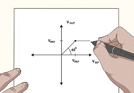
Analyse the circuit for positive input voltages. For the positive input voltages less than the Vref, the diode (Ideal) is reverse biased. Therefore, the circuit becomes open and no current flows through the circuit. In this condition, the input applied is simply reflected as output without modification. The graph is a straight line originating from the origin, having an angle of 45' with the X-axis (or Y-axis). When the input voltage exceeds the Vref, the diode (Ideal) becomes forward biased and hence it is a short circuit. The output will be equal to the magnitude of Vref. Hence, you can get a graph of a straight line from Vref point, which is parallel to the X-axis. The slope of this line is zero because, as Vinp changes, Vout does not change, but it remains constant to Vref. That is, the value of Δ Vout= Vref - Vref= 0 and the value of Δ Vinp= Vinp2 - Vinp1= b (some value). Therefore tan θ = 0/b = 0.
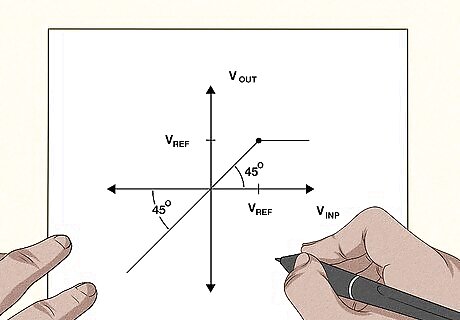
Draw the transfer characteristics. After analysing the circuit for positive and negative input voltages completely, plot the graph. Transfer characteristics for the above circuit is as shown in the figure. Observe the slope of that graph for Vinp less than Vref and more than Vref.


Comments
0 comment